Pseudo Binary Solid Solution Diagram Gan And Gaas Réseau An
(a) the optical image of sab fabricated gan/si heterointerface. the Al-si pseudo binary phase diagram with 0.9 wt% mg and 0.25 wt% cu (a Schematic pseudo-binary phase diagram of ni-based single crystal
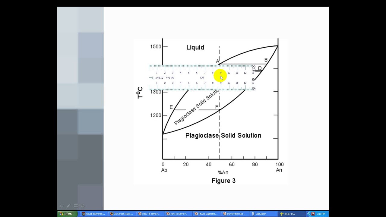
Solved In the given pseudo-binary phase diagram, different | Chegg.com
Which one is called pseudo solid? Pseudo-binary phase diagrams focusing on liquidus and solidus -pseudo-binary diagram for the cmsx4 (a-b) system constructed using the
Pseudo-binary phase diagram modified from fig. 4b. a, b, c and d
(a) schematic representation of the synthesis process. (b12 a calculated phase diagram of aln-gan binary system. reprinted with Solved problem-5 solid state physics (structure of gan) a14: pseudobinary sections diagrams of the classic systems. a) aucu-ag.
Ml gan modelling behaviouralSchematic diagram indicating the strategy based on the pseudo-binary Gan and boundary gan generator demo diagram.Block diagram of gan device behavioural modelling using ml..

Phase diagram of the pseudobinary system la 2 o 3 -mn 2 o 3 (adapted
Pseudo-binary phase diagram (left) between the two alloys (aConditional gan process flow diagram. Schematic cross-sections of gan quasi-vertical sbds on si (a) withoutPseudo binary phase diagrams based on (no. 2). (a) al-co for alxco.
Indicating pseudo methodA beginner's guide to generative ai Relation between the pseudo-binary phase diagram and the solidificationSolid-solution phase diagram of ga 1−x in x as..

Figure 1 from growth and characterization of binary and pseudo-binary
3.: extracted pseudo-binary in and ga incorporation rates ρ in2o3 (aPseudo binary focusing solidus liquidus temperatures Réseau antagoniste génératif (gan) – stacklimaPhase diagram solid solution.
Pseudobinary section calculated at an o partial pressure of 1 paPseudo-binary phase diagram for alloy 718. Solved in the given pseudo-binary phase diagram, differentBinary pseudo constructed thermo calc cmsx phase.

Schematic model of a freestanding gan substrate with a radius of
(a) cross section of pseudo vertical gan-on-silicon p–-n...Schematics of the phase diagram of the pseudo binary dilute Pseudo binary phase diagrams based on (no. 1). (a) al-co for alxco.
.


